Advanced PCB
Advanced PCB
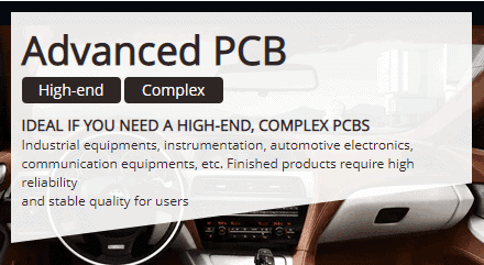
With the rapid development of technology, there is great demand on advanced PCB. Now the advanced PCB has been widely used in high-end and high precision electronic devices, such as automotive electronics, complex industrial equipment, complex computing, instrumentation, as well as communication equipment, etc.
Specialized in the advanced PCB, MUC PCB has fully updated the production equipments and fabricate your printed circuit board with the advanced technologies. What’s more,MUC PCB offers mature and high-class quick turn PCB fabrication and assembly, supported by its three PCB factories covering 15,000 square meters totally.


What PCBs . fabricated?
6-layer HDI PCB
6-layer HDI PCB
HDI-10-layers-1
32-layers Backplane-board
10-layer-Multi-layer boards
HDI-14 layers
Communication HDI
HDI-10 layers
Our 3 Guarantees

Quality
All PCBs pass the
free AOI and E-Test 100%
before they leave the factory

Speed
Prototypes take as little
as 24 hours to produce with direct DHL
or Fedex pickup at our warehouse

Support
Free DFM and next business day
replies from our highly qualified
customer support team
Submit your enquiry and get an instant quote now, or contact us about large quantities or with any questions you may have
MUC PCB Advanced PCB Capabilities
MANUFACTURING CAPABILITIES | Standard | Advanced |
CIRCUIT/PANEL SIZE | ||
Layer Count | Up to 30 | Up to 40 |
Double Side | 580*760mm | 580*890mm |
Multilayer | 570*760mm | 570*850mm |
MATERILA | ||
Standard | Shengyi/FR-4 (S1141) | |
High Tg | Shengyi/ FR-4 (S1170, S1000-2) ITEQ/IT180 | |
Halogen Free | Shengyi/S1155/S1165 | |
Special | Rogers, Taconic, Arlon | |
Plating Chemical Solutions | ROHM and HAAS | |
Others | Available on request | |
SURFACE FINISHES | ||
Standard | Leaded HASL, Lead Free HASL, ENIG, OSP, Plating Nickel/Gold,Immersion Tin, Immersion Silver | |
Selective Surface Treatment | ENIG+OSP, ENIG+Gold Finger, Immersion Tin+Gold Finger, Immersion Silver+Gold Finger | |
COPPER FOIL | ||
Base Copper thickness | 12um、18um、35um、70um、10um | |
PTH | Min. 25um | |
Inner Layer | 2 oz/ 70um | 5 oz/175um |
Outer Layer | 7 oz/245um | 10 oz/350um |
Aspect Ratio | 14:1 | 16:1 |
Finished Borad thickness/Tolerance | 0.2-7.0mm ( ≤1.0mm±0.1; >1.0mm±10%) | |
TRACE | ||
Min. Inner Layer trace width/Space | 0.10/0.10mm (Max.Cu 35um) | 0.08/0.08mm(Max.Cu 18um) |
Min. Outer Layer trace width/Space | 0.10/0.10mm (Max.Cu 35um) | 0.08/0.08mm(Max.Cu 18um) |
SOLDER MASK/SILK SCREEN | ||
Solder Mask | Black, Matte, Green, Red, Yellow,White,Blue | |
Via Filling Solder Mask/Eposy Resin | 0.65mm | 0.8mm |
Peelable Solder Mask | Yes | |
Silk Screen | White, Black, Yellow | |
CNC DRILLING | ||
Min. Finished Hole Size (Mechanical) | 0.25mm | 0.15mm |
Min. Finished Hole Size (Laser) | 0.10mm | 0.05mm |
CRITICAL TOLERANCES | ||
Layer Registration | ±0.10mm | |
Holes | ||
Hole Diameter (PTH) | ±0.075mm | ±0.050mm |
Hole Diameter (Non-PTH) | ±0.10mm | |
Hole Position | ±0.05mm | |
Slot hole (PTH) | ±0.15mm | |
General | ||
Finished PCB Thickness | 0.10mm | ±10% |
Routing Profile | ±0.15mm | ±0.10mm |
V-Cut Profile | ±0.15mm | ±0.10mm |
Warpage % | 0.70% | 0.50% |
Electrical Test % | 100% | |
OTHER OPTIONS | ||
AOI | All Multilayer | |
Impedance Control | ±10% | ±5% |
Solderability Testing | Yes | |
SPECIAL REQUIREMETNS | ||
Plated Slots | Edge Plating | |
Countersinking | Edge Bevelling | |
Others | available on request | |
